-
-
-
Design Resources
- Design & Development
- Featured Design Tools
- Partners
- Content & Training
-
Support
-
Support Forums
Get help from our expert Renesas technical staff and community.
- Technical Support
- Training & Events
- Quality & Packaging
-
Support Forums
-
Sample & Buy
-
Buy Direct from Renesas
Customers can now choose the convenience of buying direct from Renesas.
- Ordering Resources
-
Buy Direct from Renesas
9DB233
circleActiveSamples Available2-output 3.3 V PCIe Gen1-2-3 Zero Delay / Fanout Buffer
Overview
Description
The 9DB233 zero-delay buffer supports PCIe Gen3 requirements, while being backwards compatible to PCIe Gen2 and Gen1. The 9DB233 is driven by a differential SRC output pair from an IDT 932S421 or 932SQ420 or equivalent main clock generator. It attenuates jitter on the input clock and has a selectable PLL bandwidth to maximize performance in systems with or without Spread-Spectrum clocking. An SMBus interface allows control of the PLL bandwidth and bypass options, while 2 clock request (OE#) pins make the 9DB233 suitable for Express Card applications.
Features
- 2- 0.7 V HCSL differential output pairs
- Phase jitter: PCIe Gen3 < 1 ps rms
- Phase jitter: PCIe Gen2 < 3.1 ps rms
- Phase jitter: PCIe Gen1 < 86 ps peak to peak
- Supports zero delay buffer mode and fanout mode
- Bandwidth programming available
- 33-110 MHz operation in PLL mode
- 10-110 MHz operation in Bypass mode
Comparison
Applications
Design & Development
Models
ECAD Models
Schematic symbols, PCB footprints, and 3D CAD models from SamacSys can be found by clicking on products in the Product Options table. If a symbol or model isn't available, it can be requested directly from the website.

Product Options
Pkg. Type |
Lead Count (#) |
Temp. Grade |
Pb (Lead) Free |
Carrier Type |
Moisture Sensitivity Level (MSL) |
Price (USD) | 1ku |
Buy / Sample |
|
|---|---|---|---|---|---|---|---|---|
| Part Number | ||||||||
9DB233AGILF circleActive Samples Available |
TSSOP | 20 | I | Yes | Tube | 1 | Get Samples, | |
| TSSOP | 20 | I | Yes | Reel | 1 | 2.658 | ||
9DB233AGLF circleActive Samples Available |
TSSOP | 20 | C | Yes | Tube | 1 | 2.95 | Get Samples, |
| TSSOP | 20 | C | Yes | Reel | 1 | 2.488 |

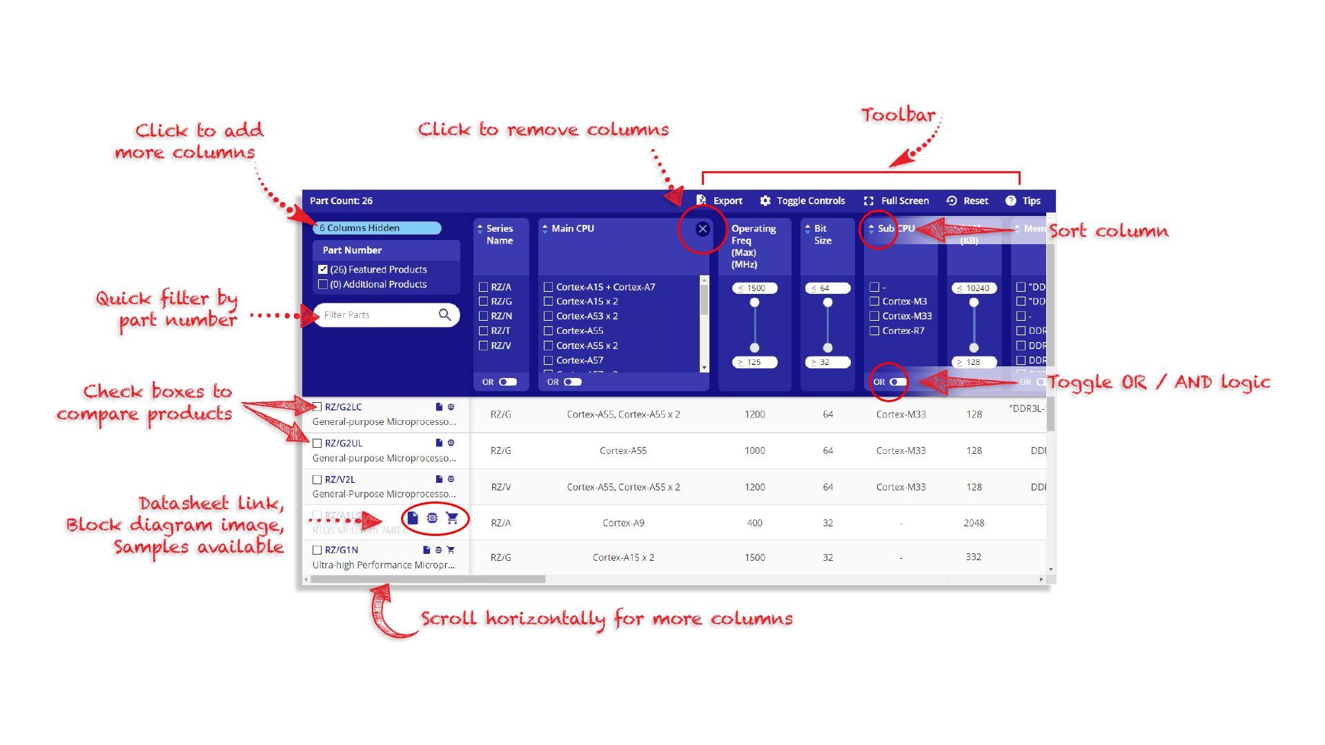
Tips for Using This Parametric Table:
- Hide Filters button in header: Collapse or expands filters
- Column sort buttons in header: Sort Column alphabetically / numerically descending or ascending
- Reset button in header: Reset all filters to the page default
- Full Screen button in header: Expand the table to full screen view (user must close out of full screen before they can interact with rest of page)
- Export button in header: Export the filtered results of the table to an Excel document
- Filter parts search bar in header: Type to filter table results by part number
- Hide column button in column headers: Select to hide columns in table
- AND / OR toggle switches in header: Toggles the logic of this particular filter to be “AND” or “OR” logic for filtering results
- Multiselect checkboxes at beginning of each row in table: Select these checkboxes to compare products against each other
- Document icon next to product name in row: View the featured document for this product
- Chip icon next to the right of the document icon in row: View the block diagram for this product
- Cart icon to the right of the chip icon: Indicates that samples are available for this product


